There are a few ways that a builder can approach the assembly of the CRX1. The recommended option is to follow the assembly guide presented below, which will take you through each stage of the CRX1 individually, and provides a number of checks to ensure proper operation. The other way is to follow the BOM and install all components of each individual type at the same time. This option is more suitable for confident and experienced builders. If you aren’t sure what you can handle, stay with the assembly guide.
When following the assembly guide, work through each section in the order presented below. At the beginning of each section, you will see an image of the CRX1 circuit board with the location of all of those section’s components highlighted. Take your time building the kit. Ensure that you have selected the correct component before soldering it to the PCB, as many of the components have no identifying markings.
Since many of the SMT components are not marked (such as the capacitors and diodes) or may come from differing manufacturers with different marking codes (such as transistors), it is very important to keep your components organized during the build. It is recommended that you do this by keeping each strip of components in the labeled compartments in their packaging. Cut off one end of the packaging to get access to the components. Only ever remove one strip of components at a time, and be sure to replace that strip into the proper compartment after using it. This will ensure that you have no mix-ups during your build.
With the preliminaries out of the way, let’s get building!
Power Conditioning
- R27 (100k)
- Q9 (IRLML9301)
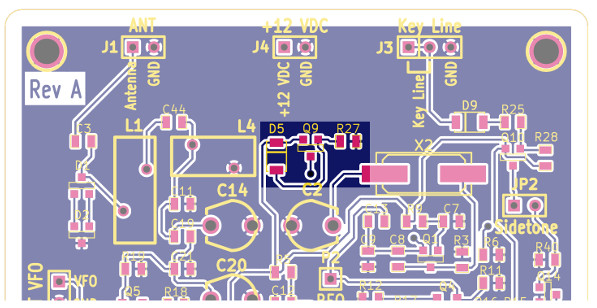
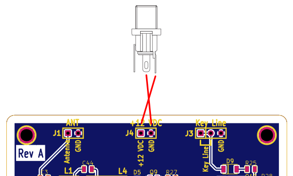
- D5 (BZV55-B15) Align the black stripe on the body of the diode with the silkscreened stripe on the PCB J4 (2.1 mm DC barrel jack) You may wish to only temporarily tack solder this jack into place so that it can be removed for convenience after checks. Using 2 lengths of hook-up wire or a 2-conductor cable, solder the DC power jack to the pads on the PCB shown below. Be sure that the “+12 VDC” pad is connected to the terminal that connects to the center pin of the jack (check continuity from the center pin to the pad on the PCB if you are unsure).
Audio Amplifier
- R48, R49 (2.2)
- R33 (470)
- R47 (47)
- R34, R45 (4.7k)
- R38 (3.3k)
- R31, R39 (10k)
- R30 (47k)
- R35 (2.2k)
- C36 (10n)
- C31 (100n)
- C32, C35, C37 (1u MLCC)
- Q11, Q15, Q16 (MMBT4401)
- Q12, Q17 (MMBT4403)
- D7, D8 (LL4148)
Align the black stripe on the body of the diode with the silkscreened stripe on the PCB
- C34 (10u electrolytic)
Align the beveled end of the capacitor base with the corresponding indication on the PCB silkscreen
- C42, C43 (100u electrolytic)
Align the beveled end of the capacitor base with the corresponding indication on the PCB silkscreen
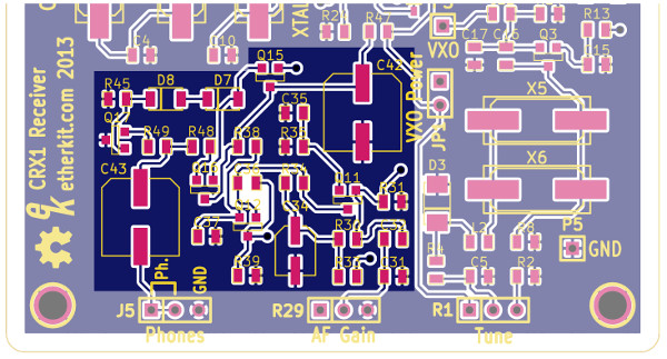
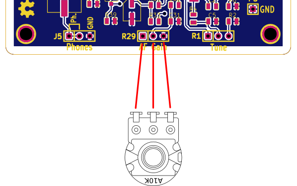
- R29 (10k audio pot)
You may wish to only temporarily tack solder this potentiometer into place so that it can be removed for convenience after the check. Locate the potentiometer labeled “A10K” on the side of the body where the shaft is located. Using 3 lengths of hook-up wire or a 3-conductor cable, solder the potentiometer to the pads on the PCB shown below.
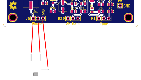
- J5 (3.5 mm stereo jack)
You may wish to only temporarily tack solder this jack into place so that it can be removed for convenience after the check. Using 3 lengths of hook-up wire or a 3-conductor cable, solder the jack to the pads on the PCB shown below.
Check
Connect headphones to J5 and set R29 to fully-counterclockwise. Apply power to the CRX1 via J3 and put your headphones on. Place a finger on the wiper of R29 (the center terminal), then slowly turn the control clockwise. You should hear some low-frequency hum before turning the control fully-clockwise. The hum should be gone when your finger is removed from the wiper of R29.
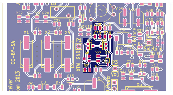
Sidetone Oscillator
- R42 (1k)
- R43 (3.3k)
- R32, R37 (10k)
- R41, R46 (4.7k)
- R44 (680)
- R40 (100k)
- C38, C39, C40, C41 (100n)
- C33 (1u MLCC)
- D6 (BZV55-B3V3)
- Q13 (MMBT4401)
- Q14 (2N7002)
- R36 (1k trim)
- JP2
Use a small piece of solid hookup wire to connect the jumper pads. Alternately, you may substitute a 0.1” x2 header strip and use a jumper block if you think you may experiment with disabling the sidetone often.
Keying
- R25, R28 (22k)
- Q10 (MMBT4403)
- D9 (LL4148) - Not in beta
Align the black stripe on the body of the diode with the silkscreened stripe on the PCB
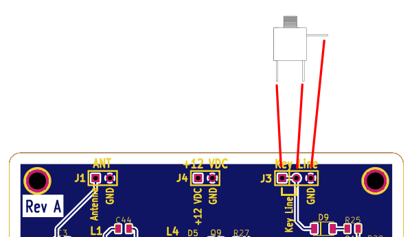
- J3 (3.5 mm stereo jack)
You may wish to only temporarily tack solder this jack into place so that it can be removed for convenience after the check. Using 3 lengths of hook-up wire or a 3-conductor cable, solder the jack to the pads on the PCB shown below.
Check
Connect headphones to J5 and a straight key to J3 (alternately, you can temporarily use a jumper wire to ground the key line at J3 for this check). Apply power to J4, then apply key down to J3. That should produce an audible sidetone at about 600 Hz in you headphones. Use R36 to adjust the sidetone level to your liking. Alternately, you can also use an oscilloscope to monitor the sidetone waveform at P4 to confirm that it is working correctly.
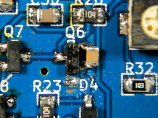
Mute
- R23, R24, R26 (100k)
- C29, C30 (1u MLCC)
- D4 (BAT46W)
Align the white stripe on the body of the diode with the silkscreened stripe on the PCB
- Q6, Q7, Q8 (2N7002)
- C45 (100n)
C45 was added to the circuit after the Rev A printed circuit boards were manufactured. Therefore, if you have a Rev A PCB, you will have to fit C45 on the same pads as the gate and source pads of Q6. There is room for this capacitor, so this is not too difficult to accomplish. Add a large blob of solder to one of the pads, then melt the solder with your soldering iron while placing C45 in place across the two pads. Keep C45 stable while removing the soldering iron, allowing the solder joint to cool. Once it has solidified, solder the other end of C45 to the other pad of Q6. The photo below shows the positioning of C45.
Product Detector
- R15 (47)
- R16 (1k)
- R17 (470)
- R11, R12 (2.2k)
- C26 (10n)
- Q4 (BF998)
Be certain to take ESD precautions with Q4, it is very static sensitive. There is a one pad on the BF998 that is larger than the rest. This aligns with the larger pad on the PCB footprint.
- C23, C25 (10u electrolytic)
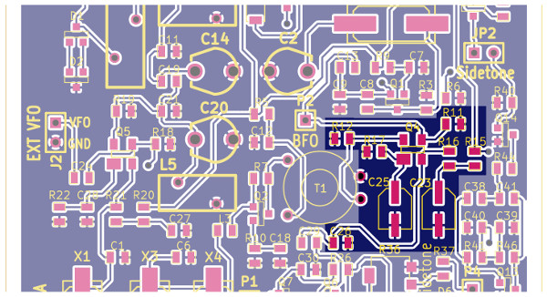
BFO
- R9 (47)
- R3 (100k)
- R6 (2.2k)
- C13 (22)
- C8, C9 (33)
- C7 (100n)
- Q1 (MMBFJ310)
- X2 (4.032 crystal)
- C2 (45 trim)
Check (Optional)
If you have an oscilloscope, you can check for the presence of the BFO signal by probing P2. The signal should be near 5 to 6 Vpp in amplitude and at a frequency near 4.032 MHz.
IF Amplifier
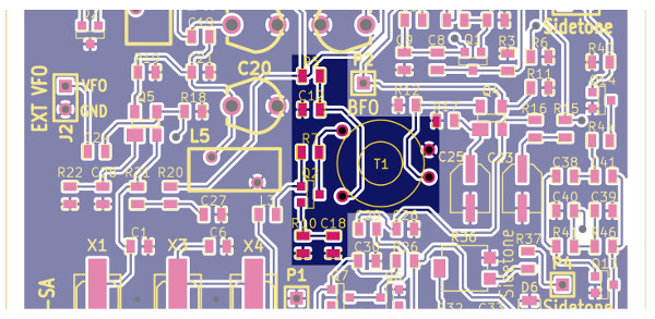
- R5 (47)
- R7 (100k)
- R10 (1k)
- C12, C18 (100n)
- Q2 (MMBT4401)
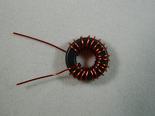
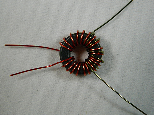
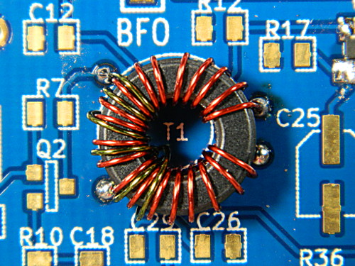
- T1 (FT37-43 6T:20T, gray toroidal core, cut 12 in/31 cm of red magnet wire for the 20T secondary, 5 in/13 cm of green magnet wire for the 6T primary)
Use the red magnet wire to wind the 20-turn secondary on the gray toroidal core, as shown below. (See the Toroidal Inductor Winding Instructions if you are unfamiliar with how to wind a toroidal inductor)
Next, use the green magnet wire to wind the 6-turn primary winding on the opposite side of the core as the secondary winding. The following illustration will show what the correct winding will look like.
Install T1 on the PCB so that the leads of the red secondary winding point towards the right side of the PCB (as viewed with the “T1” silkscreen nomenclature oriented properly) and that the green primary winding leads point towards the left. To help in identification, the pair of plated holes for the secondary leads will be spaced closer together than the holes for the primary winding.
IF Filter
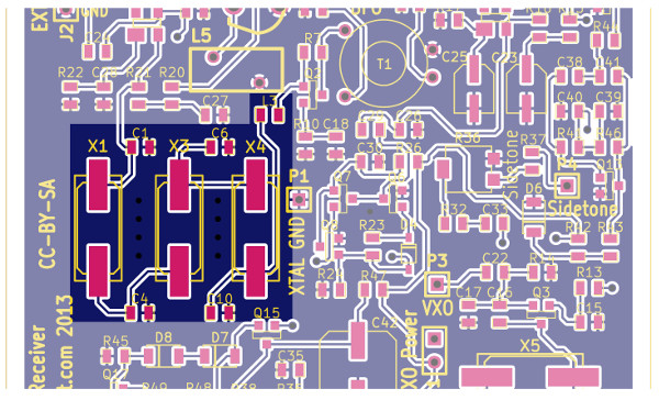
- L3 (10u)
- C1 (39)
- C4, C6 (68)
- C10 (220)
- X1, X3, X4 (4.032 MHz crystal)
Mixer
- R20 (47)
- R21 (1k)
- R19 (4.7k)
- R22 (470)
- R18 (100k)
- C24, C27, C28 (100n)
- Q5 (BF998)
Be certain to take ESD precautions with Q5, it is very static sensitive. There is a one pad on the BF998 that is larger than the rest. This aligns with the larger pad on the PCB footprint.
Bandpass Filter
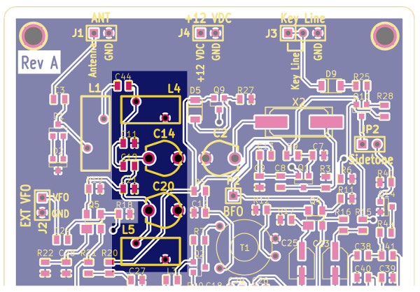
- C11 (100)
- C19 (4.7)
- C21 (150)
- C44 (47) - Not in beta
- L4, L5 (T37-2 25T, red core, cut 15 in/37 cm of red magnet wire)
(See the Toroidal Inductor Winding Instructions if you are unfamiliar with how to wind a toroidal inductor)
- C14, C20 (45 trim)
T/R Switch
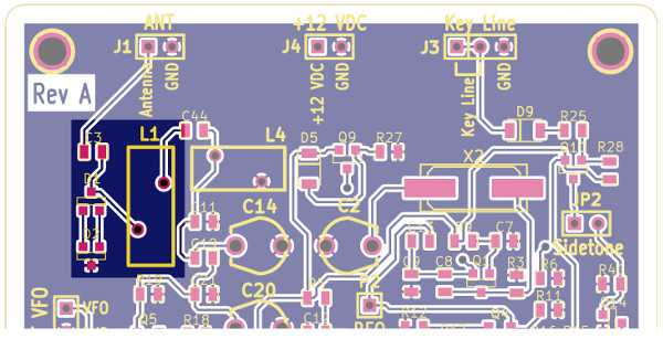
- C3 (47)
- D1, D2 (BAV99)
- L1 (T50-2 47T, large red core, cut 33 in/84 cm of red magnet wire)
(See the Toroidal Inductor Winding Instructions if you are unfamiliar with how to wind a toroidal inductor)
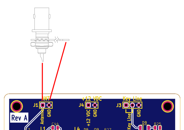
- J1 (BNC)
Using 2 lengths of hook-up wire or a 2-conductor cable, solder the BNC jack to the pads on the PCB shown below.
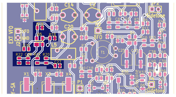
VXO
- R13 (47)
- R4, R8 (100k)
- R14 (680)
- R2 (3.3k)
- L2 (1u)
- C16, C17 (68)
- C5, C15, C22 (100n)
- Q3 (MMBFJ310)
- D3 (GS1M)
Align the white stripe on the body of the diode with the silkscreened stripe on the PCB
- JP1
Use a small piece of solid hookup wire to connect the jumper pads. Alternately, you may substitute a 0.1” x2 header strip and use a jumper block if you think you may experiment with disabling the VXO often.
- X5, X6 (11.059 crystal)
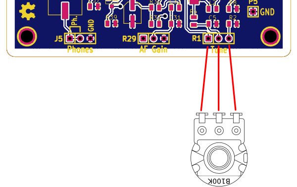
- R1 (100k linear pot)
Locate the potentiometer labeled “B100K” on the side of the body where the shaft is located. Using 3 lengths of hook-up wire or a 3-conductor cable, solder the potentiometer to the pads on the PCB shown below.
Alignment and Final Check
Alignment of the CRX1 is a simple affair that only takes a few moments. Connect J4 to DC power (preferably between +12 to +14 VDC), J5 to headphones, and a suitable 40 meter antenna to J1. Set AF gain control R29 to approximately half of its maximum. You should hear some band noise in the headphones.
First, peak the bandpass filter by alternately adjusting C14 and C20 until you hear maximum band noise in the headphones. It will probably take a few iterations to find the settings for maximum signal.
Next adjust C2 to set the BFO to the proper frequency for the IF filter. This can be a bit subjective, but the goal is to get maximum gain when tuned into a signal while rejecting as much of the opposite sideband as possible. If you have a signal generator for 7.030 MHz, it can be used as a test signal for this adjustment, or alternately you can use a signal off the air. Tune to the test signal for a audio tone at your preferred CW listening frequency (usually from 500 to 800 Hz). Tweak C2 for maximum signal level and most natural sounding background noise (it shouldn’t sound too muffled or too tinny). Tune to the opposite sideband with R1 to check sideband rejection. Unless you are using a very strong test signal, you should hear nothing on the opposite sideband. It may take a few iterations of this process to find the optimum BFO point.