Building the Si5351A Breakout Board is a relatively simple affair, but you will probably want to have a copy of the schematics handy while you are assembling the kit.
Since many of the SMT components are not marked (such as the capacitors) or may come from differing manufacturers with different marking codes (such as transistors), it is very important to keep your components organized during the build. It is recommended that you do this by keeping each strip of components in the labeled compartments in their packaging. Cut off one end of the packaging to get access to the components. Only ever remove one strip of components at a time, and be sure to replace that strip into the proper compartment after using it. This will ensure that you have no mix-ups during your build.
Assembly
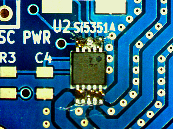
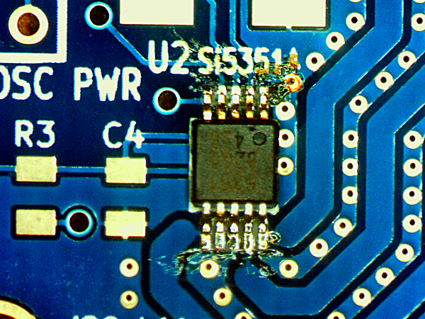
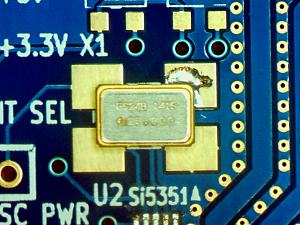
- U2 - Si5351A This IC is a MSOP-10 package, which has a fairly small lead pitch, but actually is not terribly difficult to solder to the board.
We apologize; on the first production run of PCBs, the U2 index mark was inadvertently left off the silkscreen layer by the manufacturer. Please note that the pin 1 index (the round indentation) is oriented towards the legend “U2 Si5351A” (or towards the top of the PCB if you are holding it in the orientation to read the text on the PCB).
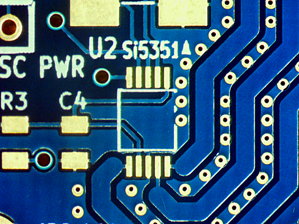
Start by applying a small bit of solder to one of the corner pads.
Tack down the IC by placing it on the component footprint and reflowing the solder onto the corner pin.
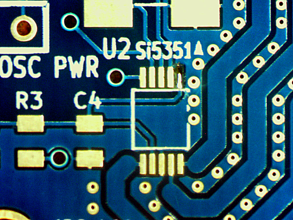
Making sure that the pins on both sides of the IC stay aligned with the footprint, solder all of the other pins on the same side. It is perfectly fine (and probably inevitable) that there will be solder bridges between pins. We will correct that a bit later.
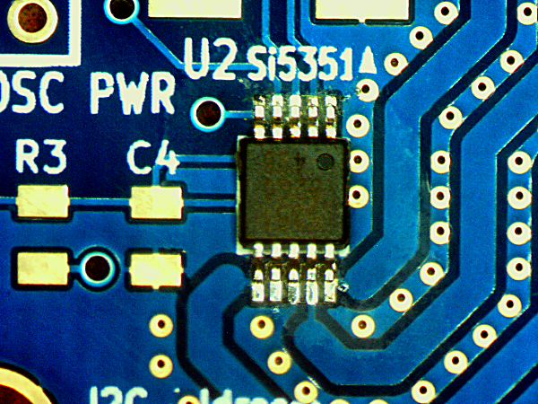
Apply solder in the same way to all of the pins on the other side of the IC.
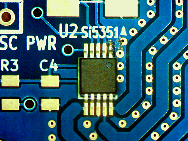
Now lay a strip of desoldering wick across one row of pins.
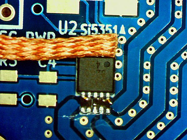
Use your soldering iron to wick up all of the excess solder. Make sure that no solder bridges remain.
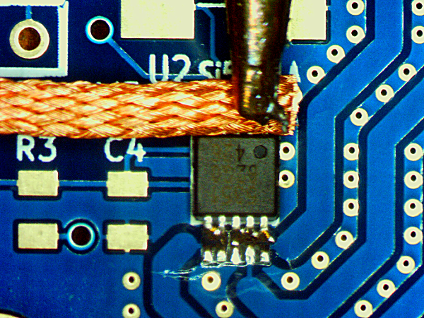
Repeat the desoldering wick procedure on the opposite side of the IC.
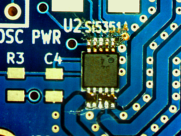
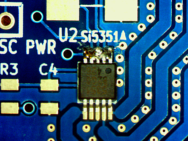
Here is the result of the previous operation done correctly. Note that there are no solder bridges and it looks like almost all of the solder is gone. However, you can check that the IC is still soldered down by using a small pick to gently push on the pins if you are uncertain. Be very careful if you do this; the pins of the IC are quite fragile and can break off easily!
One the flux has been removed, you can see that the soldering looks quite nice, considering the simple tools used. For removing flux here, we used toothbrush dipped in 99% isopropyl alcohol (IPA), followed by a brush with some water to remove any IPA residue. Be sure to let your PCB dry completely before applying power!
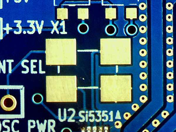
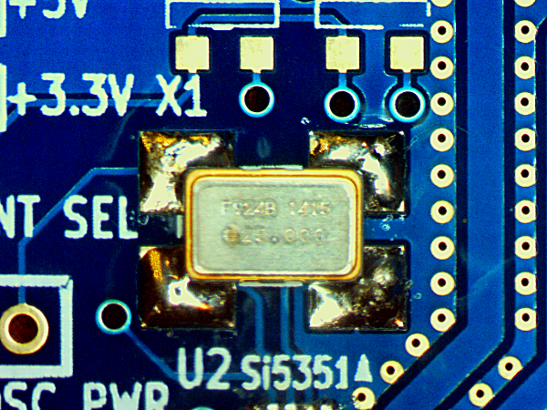
- X1 - FOX924B-25.000 or ECS-250-8-30B-CKM
If you are using the FOX924B-25.000 TCXO, then the orientation of the component matters. Please be sure to align pin 1 of the FOX924B-25.000 (which is indicated by the circle) towards the bottom-left corner of the footprint (when viewed with the PCB oriented so that you can read the text). If you are using the ECS-250-8-30B-CKM crystal, then the component can be oriented other up or down.
We apologize; on the first production run of PCBs, the X1 index mark was inadvertently left off the silkscreen layer by the manufacturer. Please note that the pin 1 index (the round indentation) is oriented towards the legend “U2 Si5351A” (or towards the bottom of the PCB if you are holding it in the orientation to read the text on the PCB).
Start by applying a bit of solder to one of the pads to use as an anchor point.
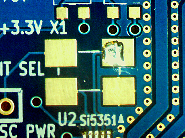
Place X1 on the footprint in the correct orientation, and while holding it in place, use your soldering iron to reflow the solder on the pad so that the component is soldered to the pad.
Now solder the other three pads. Note that the X1 has contacts both on the bottom and on the corners of the component. Make sure to flow solder onto that corner pad in order to make a good connection.
- Q1, Q2 - 2N7002
- U1 - LP2985-3.3 You may wish to use a technique similar to that used with U2 on this IC.
- C2, C4 - 100 nF
- C1 - 1 uF MLCC
- C3 - 4.7 uF MLCC
- R1, R2, R3, R4 - 10 kΩ
-
J1, J2, J3 - 0.1” headers Your kit comes with one 11-pin strip. Clip off two 3-pin headers with diagonal cutters.
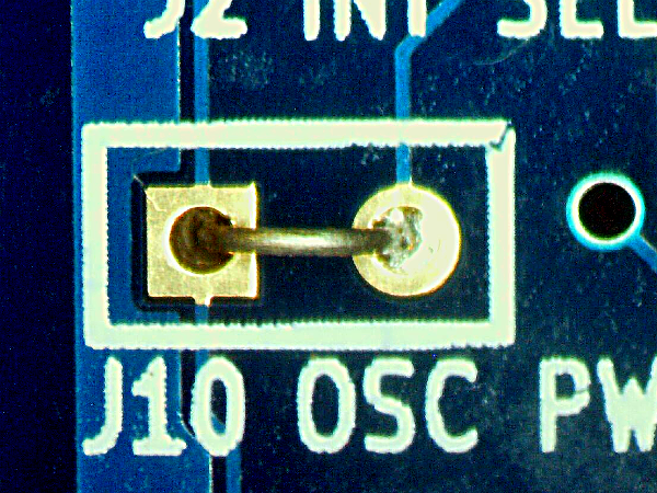
- J10 If you have the standard kit (with the ECS-250-8-30B-CKM crystal), then leave this jumper as is.
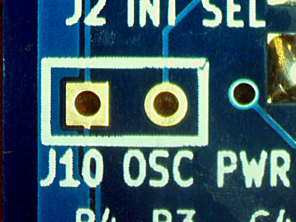
If you have the TCXO kit (with the FOX924B-25.000), then install a bit of jumper wire between the two pads of J10 to apply power to X1.
- J4, J5, J6 - SMA female end-launch (optional)